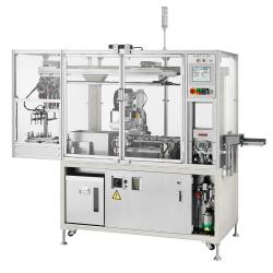
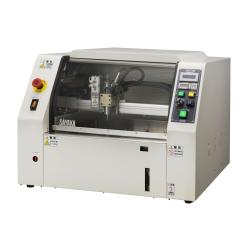
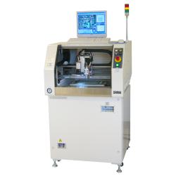
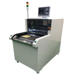
Sayaka PCB Router: Methods of PCB Depaneling and Mechanical Stress
Commonly used PCB depaneling methods are; a)hand- breaking with V-groove or perforation, b)rolling blade with V-groove, c)die cutting, and d)router depaneling. Hand breaking by operator is the simplest and least costly method; however, bending the PCB until it cracks generates great stress on the board and components. In addition, the quality of the process is operator dependent. The rolling blade method is a relatively low cost and fast process but a high level of stress occurs at the cut point of the PCB. Die cutting method generates less stress on a PCB supported by dies but requires a set of costly dies designed for the particular PCB. Router depaneling generates the least amount of stress at depaneling although it has been previously known as a slow process, less user-friendly with programming and a high residual dust generator.
Table 1 shows the difference in stress levels by various depaneling methods. Rolling blade depaneling generates more stress than other methods. Stress level is higher in the perpendicular to cut direction with all depaneling methods.
Table 2 shows stress level by distance from cut. Obviously, the further the distance from the cut, the lower the stress level.
These test results match the PCB design recommendation by chip component manufacturers. Fragile chip components should be mounted 1) parallel to depaneling direction, 2) further from a cutting tab and V-groove. With all test conditions, router depaneling generates the least amount of stress.
Table 1. Stress level comparison by depaneling methods
| Depaneling method | Direction | Stress level | ref. Stress limit of Ceramic capacitor |
|---|---|---|---|
| Hand breaking with V-groove | Parallel to cut | 400µƐ | 800 to 1800µƐ |
| perpendicular to cut | 1800µƐ | ||
| Rolling blade with V-groove | Parallel to cut | 1700µƐ | |
| perpendicular to cut | 1600µƐ | ||
| Router (1.0mm bit, 10mm/sec) | Parallel to cut | 110µƐ | |
| perpendicular to cut | 300µƐ |
* Sample PCB: CEM3, T = 1.6mm
Table2. Stress level comparison by distance form cut
| Depaneling method | Distance form cut | Stress level | ref. Stress limit of Ceramic capacitor |
|---|---|---|---|
| Rolling blade with V-groove | 3mm | 1500µƐ | 800 to 1800µƐ |
| 4mm | 500µƐ | ||
| Router (1.2mm bit, 15mm/sec) | 3mm | 60µƐ |
* Sample PCB: Glass-Epoxy, T = 1.2mm
* Refer to the Appendix for Test Condition
APPENDIX
Stress Test Condition and Test Data
Strain gauge: KFG-2-120-L1-11L1M2R (Kyowa Electronic Instruments Co. Ltd.)
Amplifier: DPM-712B (Kyowa Electronic Instruments Co. Ltd.)
Strainmeter: HIOKI 8804
Sample PCB: Glass-Epoxy 1.2mm thickness with V-groove Rolling Blade: Titanium plated two disc cutter, feeding speed 100mm/sec
Router bit: Tungsten alloy 1.2mm diameter, feeding speed 15mm/sec
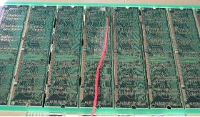
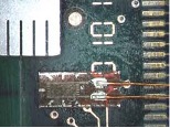
Fig. 10 Sample PCB
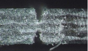
Fig. 11 PCB Cross Section
Fig. 12 Strain gauge settings
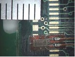
4mm from cut
3mm from cut
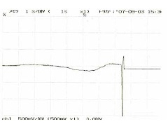
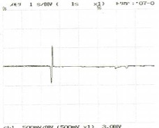
Fig. 13 Test Data
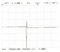
Rolling Blade (gauge 3mm from cut)
Rolling Blade2 (gauge 3mm from cut)
Rolling Blade (gauge 4mm from cut)
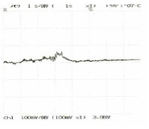
Router (gauge 3mm from cut)